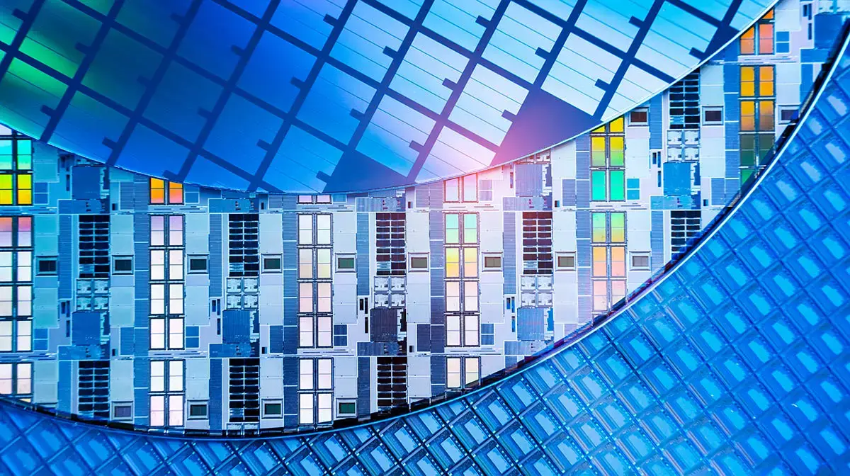
In the fast-evolving world of semiconductor manufacturing, precision and efficiency are paramount.
As device features continue to shrink, traditional fabrication methods struggle to meet the demand for finer structures, higher throughput, and minimal material waste. This is where laser micromachining plays a crucial role.
Laser micromachining enables the fabrication of intricate patterns, microstructures, and precise modifications at a scale that conventional mechanical and chemical processes cannot achieve. Whether used for drilling microvias, cutting fragile substrates, or refining photolithographic techniques, laser technology has become an indispensable tool for semiconductor manufacturers aiming to maintain cutting-edge performance and efficiency.
LASER MICROMACHINING IN SEMICONDUCTOR FABRICATION
Laser micromachining is a non-contact, highly controlled process that utilizes focused laser beams to precisely remove or modify material at the microscale. The benefits of this technology in semiconductor manufacturing include:
- High Precision: Lasers can achieve micron and sub-micron feature sizes, critical for advanced semiconductor components.
- Non-Contact Processing: Unlike mechanical tools, lasers apply no physical force, reducing stress and eliminating tool wear.
- Minimal Thermal Impact: Ultrafast laser pulses minimize heat diffusion, preventing damage to delicate semiconductor structures.
- Material Versatility: Lasers can machine silicon, compound semiconductors, ceramics, polymers, and metals with minimal contamination.
- Scalability & Automation: Laser micromachining integrates seamlessly into high-volume manufacturing lines, enhancing throughput and yield.
By leveraging these capabilities, semiconductor manufacturers can optimize production efficiency, reduce defects, and maintain compliance with stringent quality standards.
APPLICATIONS OF LASER MICROMACHINING IN SEMICONDUCTOR MANUFACTURING
Laser Drilling & Microvia Formation
Semiconductor devices require microvias - tiny interconnect holes that facilitate electrical connections between layers. Laser micromachining provides an optimal solution for drilling these features with:
- High Aspect Ratios: Ultrafast lasers create deep, narrow holes necessary for multi-layered semiconductor packaging.
- Selective Material Removal: Laser drilling ensures precise hole placement and diameter control across diverse substrates.
- Enhanced Cleanliness: Minimal debris and burr-free hole edges improve circuit reliability.
Laser Annealing: Enhancing Semiconductor Performance
After ion implantation, semiconductor wafers require thermal treatment to activate dopants and restore crystal integrity. Laser annealing offers localized, rapid thermal processing with minimal wafer warping. This technique is essential for:
- Ultra-Shallow Junction Formation: Enabling smaller, more efficient transistors.
- Stress Reduction: Improving semiconductor reliability by minimizing thermal strain.
- Selective Activation: Adjusting electrical properties without excessive heat diffusion.
Laser Trimming: Precision Calibration of Semiconductor Components
Many analog and mixed-signal semiconductor devices require post-fabrication tuning. Laser trimming enables real-time adjustment of resistor, capacitor, and sensor values by selectively removing material.
This highly controlled process ensures that each semiconductor device meets strict performance specifications, reducing variability and improving overall yield.
Laser Marking for Traceability
Laser marking is widely used in semiconductor manufacturing for component identification and traceability. By engraving serial numbers, barcodes, and QR codes on wafers and chips, manufacturers ensure quality control and compliance with industry regulations.
TECHNOLOGICAL ADVANCEMENTS IN LASER MICROMACHINING
Ultrafast Lasers for Next-Gen Semiconductor Processing
The introduction of femtosecond and picosecond lasers has revolutionized semiconductor manufacturing. These ultrafast lasers offer:
- Minimal Heat-Affected Zones: Reducing thermal damage to sensitive microstructures.
- Higher Precision & Control: Allowing for sharper edges and improved material integrity.
- Increased Processing Speeds: Enabling high-throughput production lines.
Hybrid Laser Processing Techniques
Innovations in laser processing now integrate hybrid approaches, such as combining laser micromachining with additive manufacturing, plasma etching, and ion beam machining. This fusion of technologies enhances efficiency and broadens the range of materials that can be processed.
AI & Machine Learning in Laser Micromachining
AI-driven optimization of laser micromachining processes is an emerging trend. By utilizing machine learning algorithms, manufacturers can:
- Improve Accuracy & Consistency: Automatically adjusting laser parameters in real-time.
- Enhance Process Automation: Reducing human intervention and production costs.
- Predict & Prevent Defects: Identifying anomalies before they impact yield.
Interposer Technology for Next-Generation Integration
Interposers are key enablers in heterogeneous integration, allowing chiplets to be combined with high density and precision on silicon or glass substrates.
- Advanced Packaging Platforms: Facilitate integration of complex semiconductor components.
- Silicon & Glass Interposers: Offer high-speed interconnects and improved thermal performance.
- Critical for Chiplet Architectures: Support the move toward modular, scalable semiconductor systems.
INDUSTRY TRENDS AND MARKET GROWTH
Demand for Miniaturization & Advanced Packaging
The semiconductor industry is shifting toward smaller, more powerful chips for 5G, AI, and IoT applications. This has led to increased adoption of advanced packaging techniques, where laser micromachining plays a crucial role in creating ultra-fine interconnects and microvias.
Sustainability in Semiconductor Manufacturing
Environmental considerations are driving the adoption of energy-efficient laser technologies that reduce material waste and hazardous chemical usage. Laser-based dry processing techniques help meet regulatory compliance for green manufacturing initiatives.
ADVANCE YOUR SEMICONDUCTOR MANUFACTURING WITH OPTEK SYSTEMS
As semiconductor technology continues to evolve, the demand for high-precision, scalable manufacturing processes grows. OpTek Systems provides the expertise, technology, and support needed to drive innovation in semiconductor fabrication. Our laser micromachining solutions are designed to meet the highest industry standards, ensuring optimal performance and efficiency.
To learn how OpTek Systems can enhance your semiconductor manufacturing processes, contact us today and explore the possibilities of precision laser micromachining.