We provide advanced laser processing tools for precision machining of conducting, insulating, and semiconductor materials.
The electronics sector is among the best placed to exploit the advantages of precision laser micromachining. With large volumes of tiny components, constructed from a combination of electrically conducting and insulating materials, substrates in a variety of materials, such as glass-reinforced epoxy, Kapton, and ceramic that require cutting and drilling, and multilayer or coated materials that require patterning.
The versatility of laser processing provides precision manufacturing processes across electronics, including flexible/plastic electronics, microelectronics, and semiconductor applications. Typical examples include:
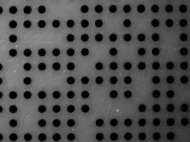
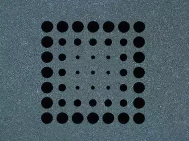
- Tools for cutting and drilling a range of PCB materials, with straight and shaped profiles and via diameters down to a few 10’s microns
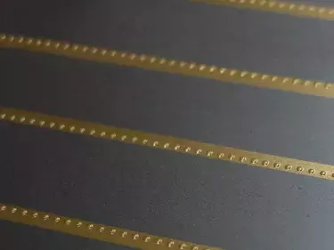
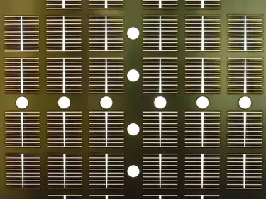
- Systems for patterning metalized films in the production of small form factor, thin film capacitors
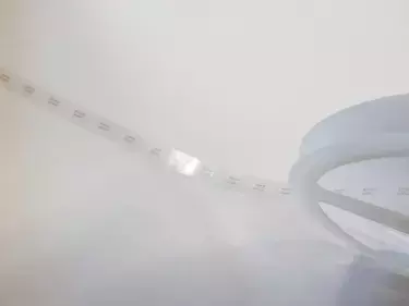
- Automated tools for high volume processing of surface mount capacitors, to remove excess potting material from the electrical connections
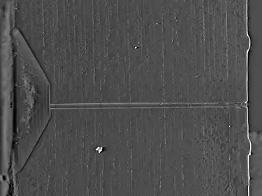
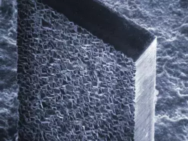
- Equipment for dicing thin plastic die and releasing the die from the glass carrier that is used to stabilize the film during the printing/coating processes
- Systems for precision targeting of laser PROM structures for hard coding memory at the individual device level
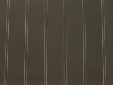
- Laser patterning of conductive coatings to create electrical circuits, fanouts and devices like RF antennae
- Precision cutting of printed/coated, multilayer electrochemical sensors to expose the full sensor cross-sectional area
- Annealing of nanoparticle inks and coating to maximize conductivity in precise paths and regions
Need our help? Fill out our form to ask our OpTek experts.