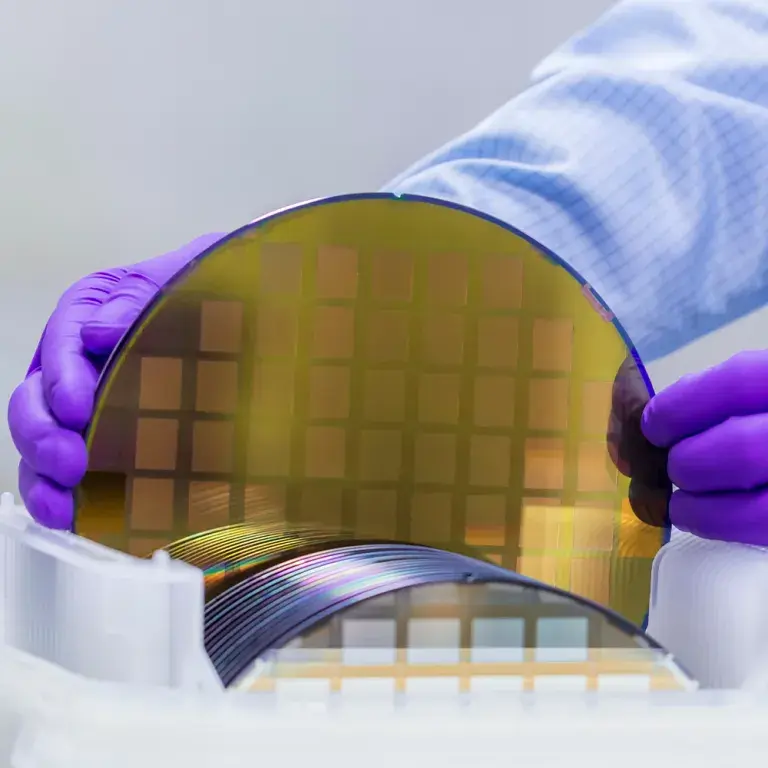
Laser scribing is a vital process in advanced manufacturing environments where accuracy, yield optimization, and material integrity are critical.
By employing controlled laser ablation to generate defined scribe lines on a substrate’s surface, manufacturers can achieve clean, reliable separation without the mechanical stress or contamination typical of traditional techniques. This non-contact method has become an essential enabler in sectors such as photovoltaics, solid-state lighting, microelectronics, and high-performance ceramics.
Advantages over traditional scribing methods
Unlike conventional mechanical scribing, where physical tools introduce variability, debris, and stress; laser scribing uses finely focused energy to remove only a surface layer of material.
This action weakens the structure along a defined path, allowing for downstream separation through cleaving, snapping, or peeling with remarkable consistency. Because the process avoids direct contact with the substrate, there is no tool wear, no risk of particulate contamination, and significantly reduced sub-surface damage. Furthermore, it facilitates tight dimensional control with scribe widths often below 30 microns, and in certain applications, as narrow as 5 microns.
Traditional scribing techniques, such as mechanical scribing using diamond-tipped tools, have several limitations:
- Mechanical Stress: Physical contact can introduce micro-cracks and stress points, leading to material damage.
- Limited Precision: Mechanical methods may lack the fine control needed for intricate patterns or delicate materials.
- Tool Wear: Contact-based tools degrade over time, affecting consistency and increasing maintenance costs.
In contrast, laser scribing offers:
- Non-Contact Processing: Eliminates mechanical stress, reducing the risk of damage.
- High Precision: Enables the creation of intricate patterns with micron-level accuracy.
- Versatility: Suitable for a wide range of materials, including metals, ceramics, glass, and polymers.
- Reduced Contamination: Minimizes debris and contamination, essential for cleanroom environments.
Applications For Laser Scribing

PERC Solar Cells
In the fabrication of Passivated Emitter Rear Cells (PERC), laser scribing plays a critical role in defining localized contact regions on the rear surface. These solar cells incorporate dielectric passivation layers, typically silicon nitride or aluminium oxide, that enhance carrier lifetime and optical efficiency. However, for current collection to occur, these layers must be selectively removed without damaging the underlying silicon.
Laser scribing achieves this with a level of precision unattainable by mechanical or chemical means. Ablation can be tightly controlled to remove only the dielectric stack, preserving the passivation in non-contact areas and thus maximizing efficiency. Scribe widths ranging from 5 to 30 microns have been shown to deliver optimal contact formation while minimizing shading losses and preserving the thermal integrity of the substrate. As a result, manufacturers report improved power conversion efficiency and higher process repeatability when adopting laser scribing for rear-side processing of PERC architectures.
LED Wafer Scribing
LED wafer processing presents a unique set of challenges due to the optical and physical properties of the materials involved. Gallium nitride (GaN), a common emitter layer in high-brightness LEDs, is frequently deposited on sapphire substrates, materials that are partially or fully transparent to visible wavelengths. Mechanical cleaving in this context is unreliable, often resulting in uneven fractures, wafer loss, or contamination.
Laser scribing overcomes these limitations by employing specific wavelengths and pulse durations capable of coupling energy effectively into the target material. By operating in green and infrared spectral regions, the laser energy is absorbed within the transparent substrate, enabling sub-surface modification or surface ablation with minimal collateral damage. In production-scale environments, short-pulsed lasers have been successfully used to generate high-quality scribe lines, resulting in improved fracture propagation and reduced die chipping.
Empirical results from studies conducted under the U.S. Department of Energy’s solid-state lighting programs have validated the throughput and cost-efficiency gains of laser-based processing over conventional sawing methods. These benefits have underpinned the widespread adoption of laser scribing in high-volume LED manufacturing, where yield consistency and contamination control are paramount.
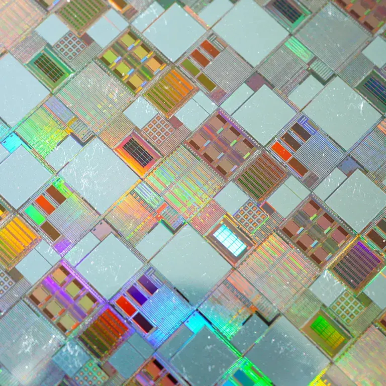
Ceramic and Silicon Wafer Scribing
Ceramic substrates and silicon wafers are widely used in microelectronics, MEMS, and advanced packaging due to their electrical insulation, thermal stability, and mechanical hardness. However, these same properties make them difficult to process using mechanical methods, which often introduce micro-cracking, delamination, or fracture unpredictability.
Laser scribing offers a precise and controllable alternative. Experiments using short nanosecond pulse lasers have demonstrated significant improvements in both scribe depth and surface integrity. In a comparative study using single 25-nanosecond pulses, the introduction of pulse shaping and burst micromachining techniques resulted in a measured ablation depth increase of up to 77%, depending on material and energy configuration. Additionally, the use of split-pulse strategies allowed for enhanced energy distribution across the scribe path, reducing localized stress and improving the cleaving behaviour post-scribing.
These capabilities are especially valuable in applications involving multilayer substrates, metallization stacks, or devices requiring narrow streets and high edge quality. By enabling precise material weakening without introducing thermal distortion, laser scribing supports tighter dimensional tolerances and superior downstream processing yields.
Laser Scribing For Advanced Manufacturing
In high-performance manufacturing, laser scribing has proven to be more than just a substitute for mechanical or chemical separation. It is a strategic process that enhances manufacturing robustness, precision, and repeatability. By minimizing particulate generation and thermal impact, it ensures compatibility with cleanroom conditions and reduces the need for secondary cleaning steps. The non-contact nature of the process eliminates tool degradation and variability, leading to longer operational uptime and reduced maintenance intervention.
Moreover, the ability to tune wavelength, pulse duration, and repetition rate provides engineers with a versatile toolkit for adapting to diverse materials and product geometries. This process agility, coupled with demonstrable improvements in yield, edge quality, and throughput, makes laser scribing a compelling choice for manufacturers focused on efficiency, reliability, and long-term cost optimization.
Optek Systems Your Partner In Precision Laser Scribing
Laser scribing is a transformative process that offers unmatched precision, flexibility, and efficiency across various industries. By partnering with OpTek Systems, you gain access to cutting-edge technology and expertise that can elevate your manufacturing capabilities. Whether you’re in semiconductors, photovoltaics, or medical devices, OpTek provides the solutions you need to stay ahead in a competitive market.
OpTek Systems stands at the forefront of laser micromachining, offering bespoke solutions tailored to your specific needs. With a global presence and decades of experience, OpTek provides:
- Advanced Technology: Utilizing ultrashort pulse lasers and state-of-the-art motion control for unparalleled precision.
- Material Versatility: Expertise in processing a broad spectrum of materials, from metals and ceramics to polymers and composites.
- Customized Solutions: Designing and integrating laser systems into your production lines for seamless operation.
- Comprehensive Services: Offering contract manufacturing, prototyping, and after-sales support to ensure your success.
OpTek’s commitment to innovation and quality makes it the ideal partner for companies seeking to leverage laser scribing for enhanced product performance and manufacturing efficiency.